- 您现在的位置:买卖IC网 > Sheet目录475 > MC13851-2400EVK (Freescale Semiconductor)IC MC13851 EVB 2400MHZ
Application Information
Table 6. Typical 1575 MHz Evaluation Board Performance (continued)
(Vcc = 2.75V, T A = 25° C )
Characteristic
Symbol
Min
Typ
Max
Unit
Output Return Loss
High Gain
Bypass
S22
—
—
-13
-18
-9
-12
dB
3.2
1960 MHz Application
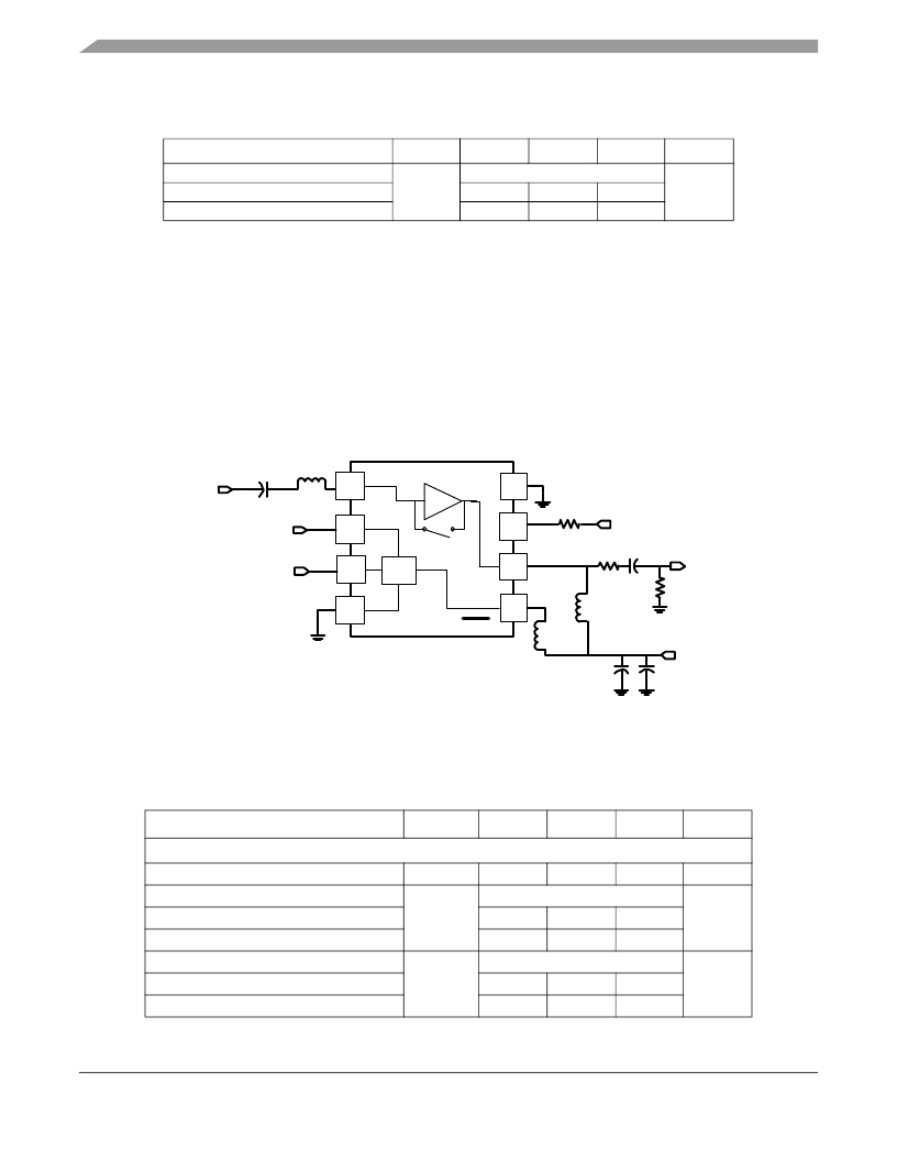
These application circuits are designed to demonstrate performance at 1960 MHz. Typical results of
NF = 1.4 dB, S21 gain > 18 dB and OIP3 of 16 dBm. Two values of bias resistor R1 are shown to
demonstrate performance for different IP3 and Icc requirements. Resistor R3 is used to de-Q output
inductor L2 and adjust gain and return losses. Inductor L3 provides bias to the logic circuit. Reducing R3
lowers gain and improves return losses. Typical performance that can be expected from this circuit at 2.75
V is listed in Table 7 .
Figure 8 is the 1960 MHz application schematic with package pinouts and the circuit component topology.
C1
2.4
L1
5.1 nH
RF IN
pF
5
4
Gnd
Enable
6
3
R1
1.2 k
R2
10
Rbias
C2
0.9 pF
Gain
7
8
Logic
2
1
L2
3.3 nH
R3
620
RF
OUT
Gnd
L3
2 70 nH
C3
33 pF
C4
.01 uF
Vcc
Figure 8. 1960 MHz Application Schematic
Table 7 shows the electrical characteristics for the 1960 MHz evaluation board.
Table 7. Typical 1960 MHz Evaluation Board Performance
(Vcc = 2.75V, Ta = 25°C)
Characteristic
Symbol
Min
Typ
Max
Unit
R1=1.2 K Ω
Frequency
f
—
1960
—
MHz
RF Gain
High Gain
Bypass
G
17.7
-6.5
18.7
-4.9
—
—
dB
Output Third Order Intercept Point
High Gain
Bypass
OIP3
14
19.2
16
20.9
—
—
dBm
MC13851 Advance Information, Rev. 2.0
12
Freescale Semiconductor
发布紧急采购,3分钟左右您将得到回复。
相关PDF资料
MC13852-900EVK
IC MC13852 EVB 900MHZ
MC13917-900EVK
IC MC13917_900_EVK
MC1496P1
IC MODULATOR/DEMODULATOR 14-DIP
MC33493MOD868EV
BOARD EVAL MC33493 TANGO
MC33591MOD315EV
BOARD EVAL MC33493 TANGO3 RF
MC33593MOD868EV
BOARD EVAL MC33593 ROMEO2 RF
MC33690DWER2
IC STAND ALONE TAG READER 20SOIC
MC44CC375AVEFEVK
CCEVK NEJA EVAL KIT
相关代理商/技术参数
MC13851EP
制造商:FREESCALE 制造商全称:Freescale Semiconductor, Inc 功能描述:General Purpose Low Noise Amplifier with Bypass Switch
MC13851EPR2
功能描述:射频放大器 Piccolo HB-Sing Band LNA RoHS:否 制造商:Skyworks Solutions, Inc. 类型:Low Noise Amplifier 工作频率:2.3 GHz to 2.8 GHz P1dB:18.5 dBm 输出截获点:37.5 dBm 功率增益类型:32 dB 噪声系数:0.85 dB 工作电源电压:5 V 电源电流:125 mA 测试频率:2.6 GHz 最大工作温度:+ 85 C 安装风格:SMD/SMT 封装 / 箱体:QFN-16 封装:Reel
MC13852
制造商:FREESCALE 制造商全称:Freescale Semiconductor, Inc 功能描述:General Purpose Low Noise Amplifier with Bypass Switch
MC13852-434EVK
功能描述:射频开发工具 MC13852 EVB 434MHZ RoHS:否 制造商:Taiyo Yuden 产品:Wireless Modules 类型:Wireless Audio 工具用于评估:WYSAAVDX7 频率: 工作电源电压:3.4 V to 5.5 V
MC13852-900EVK
功能描述:射频开发工具 MC13852 EVB 900MHZ RoHS:否 制造商:Taiyo Yuden 产品:Wireless Modules 类型:Wireless Audio 工具用于评估:WYSAAVDX7 频率: 工作电源电压:3.4 V to 5.5 V
MC13852EP
制造商:FREESCALE 制造商全称:Freescale Semiconductor, Inc 功能描述:General Purpose Low Noise Amplifier with Bypass Switch
MC13852EPR2
功能描述:射频放大器 Piccolo LB-Sing Band LNA RoHS:否 制造商:Skyworks Solutions, Inc. 类型:Low Noise Amplifier 工作频率:2.3 GHz to 2.8 GHz P1dB:18.5 dBm 输出截获点:37.5 dBm 功率增益类型:32 dB 噪声系数:0.85 dB 工作电源电压:5 V 电源电流:125 mA 测试频率:2.6 GHz 最大工作温度:+ 85 C 安装风格:SMD/SMT 封装 / 箱体:QFN-16 封装:Reel
MC13853-3B-EVK
功能描述:射频开发工具 LNA W/BYPASS SWITCH RoHS:否 制造商:Taiyo Yuden 产品:Wireless Modules 类型:Wireless Audio 工具用于评估:WYSAAVDX7 频率: 工作电源电压:3.4 V to 5.5 V
